Hexagonal Boron Nitride (h-BN): Structure, Properties, and Applications
Introduction
Boron nitride (BN) exists in several crystalline forms, including cubic (c-BN), hexagonal (h-BN), and amorphous phases. Among these, hexagonal boron nitride has attracted the most attention due to its structural similarity to graphite and its combination of thermal stability, electrical insulation, and chemical inertness. Often dubbed "white graphite," h-BN is now widely used in microelectronics, high-temperature engineering, and advanced composites.
Structure and Intrinsic Properties
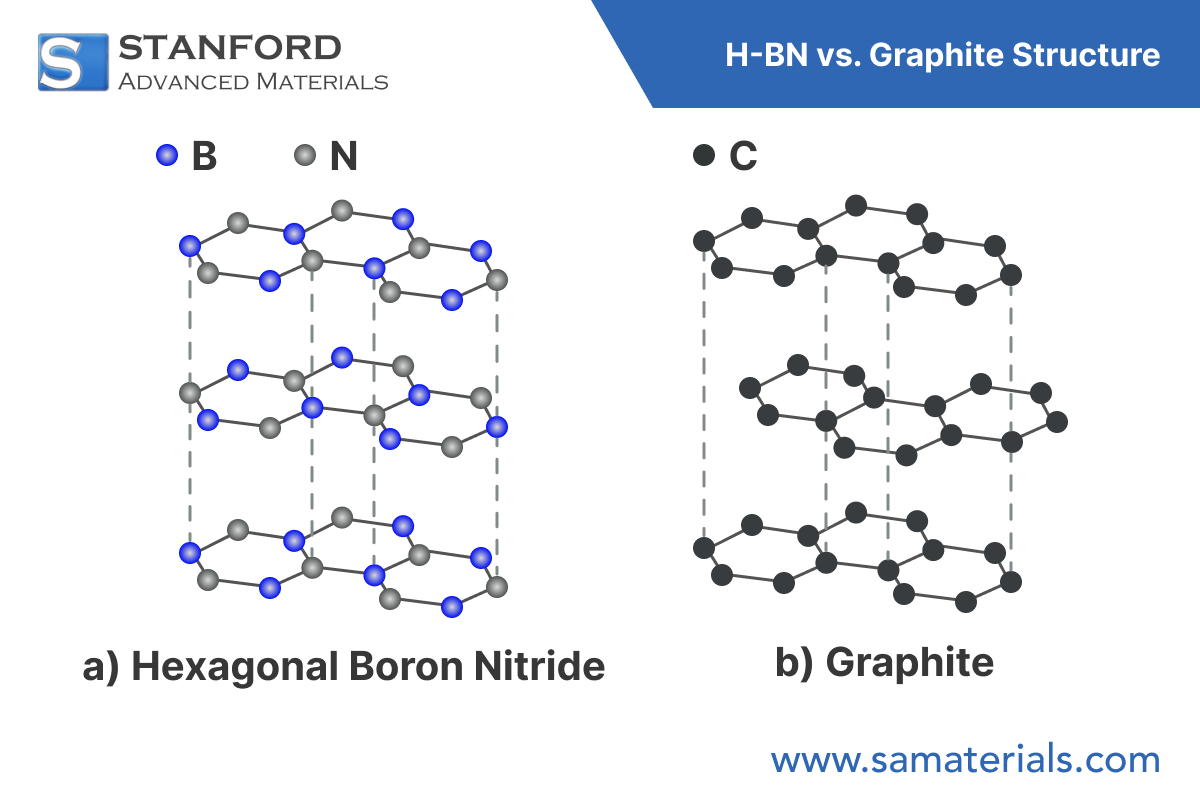
Hexagonal boron nitride adopts a layered hexagonal lattice with an ABAB stacking configuration. Each layer is composed of alternating boron and nitrogen atoms bonded by strong in-plane covalent bonds. The interlayer interaction, governed by van der Waals forces, makes the material mechanically anisotropic—stiff in-plane and easily cleavable out-of-plane.
While h-BN and graphite share a similar lattice geometry, their electronic structures differ fundamentally. Graphite is conductive due to delocalized π-electrons, whereas h-BN, with ionic B–N bonds, is a wide bandgap insulator (~5.9 eV).
Key properties:
-
Crystal structure: Hexagonal
-
Lattice parameters: a ≈ 2.50 Å, c ≈ 6.66 Å
-
Interlayer spacing: ~3.33 Å
-
Bandgap: ~5.9 eV (indirect)
-
Density: ~2.1 g/cm^3
Related Article: What Are the Characteristics of Hexagonal Boron Nitride?
Thermophysical and Chemical Properties
h-BN exhibits a unique combination of thermal conductivity, thermal stability, and chemical resistance:
-
Thermal conductivity: Up to 200–400 W/m·K in-plane; significantly lower out-of-plane.
-
Thermal expansion: Anisotropic; ~2 × 10^-6 K^-1 in-plane, higher out-of-plane.
-
Chemical stability: Inert to most acids and bases, and stable in air up to ~1000 °C.
-
Lubricity: Low friction coefficient, stable in vacuum and oxidizing environments.
These properties make h-BN suitable for demanding environments that combine heat, oxidation, and wear.
Synthesis Techniques
The synthesis route of hexagonal boron nitride (h-BN) directly determines its structural quality, lateral size, thickness control, and defect density—all of which influence its suitability in electronic, thermal, and mechanical applications. Broadly, synthesis methods can be classified into top-down exfoliation strategies and bottom-up chemical growth techniques.
Top-Down Methods
These approaches start from bulk h-BN and reduce it to thinner flakes or few-layer sheets.
Mechanical Exfoliation
This method, often referred to as the "Scotch tape" technique, involves physically peeling off layers from a bulk h-BN crystal using adhesive materials. The advantage lies in the high crystallinity and low defect density of the resulting flakes, which are ideal for fundamental studies or high-performance 2D devices. However, the process is manual, time-consuming, and inherently low-yield, making it unsuitable for large-scale or commercial production.
Liquid-Phase Exfoliation (LPE)
LPE uses ultrasonication or high-shear mixing in suitable solvents (e.g., N-methyl-2-pyrrolidone, isopropanol, or aqueous surfactant solutions) to delaminate bulk h-BN into few-layer nanosheets. It offers higher throughput than mechanical exfoliation and is scalable to gram-level or beyond. However, the process often introduces structural defects, edge oxidation, or sheet fragmentation, which can degrade electrical and mechanical properties. Centrifugation is typically used post-exfoliation to select flakes of desired thickness and size distribution.
Challenges with Top-Down Methods:
-
Control over lateral dimensions and thickness remains limited.
-
Difficult to remove surfactants or solvents completely.
-
High defect densities in LPE may limit thermal and electronic performance.
Bottom-Up Methods
Bottom-up techniques allow atomic-level control over film growth and are preferred when uniformity, thickness precision, and integration are critical.
Chemical Vapor Deposition (CVD)
CVD is the most promising method for wafer-scale synthesis of few-layer or monolayer h-BN. Common precursors include:
-
Ammonia borane (NH3–BH3): Generates BN through thermal decomposition.
-
Borazine (B3N3H6): A cyclic compound with B–N bonds already in place, yielding higher crystallinity.
-
B-trichloroborazine (B3N3Cl3) and diborane + ammonia mixtures have also been explored.
Growth typically occurs on transition metal substrates like copper, nickel, or iron foils at temperatures ranging from 900 °C to 1100 °C. The substrate type affects nucleation density, grain size, and alignment. Transfer processes are required if h-BN is to be integrated onto insulating or semiconductor surfaces.
Key parameters influencing CVD quality:
-
Precursor flow rate and purity
-
Chamber pressure (low-pressure CVD yields larger domains)
-
Substrate crystallinity and orientation
-
Cooling rate post-growth (affects grain boundary formation)
Polymer-Derived Ceramics (PDCs)
PDC synthesis involves pyrolyzing boron- and nitrogen-containing polymer precursors such as polyborazylene or poly[B-trichloroborazine]. Under a controlled atmosphere (often ammonia or nitrogen), these precursors decompose into boron nitride ceramics. This method is suited for fabricating bulk or shaped h-BN components like crucibles, insulators, or coatings. The process allows for integration with fiber reinforcements or porous scaffolds, making it ideal for structural composites.
Advantages of PDC:
-
Precise stoichiometric control
-
Custom shaping before pyrolysis
-
Ability to produce dense, non-porous ceramics for mechanical and thermal use
Summary and Trade-Offs
| Method | Crystallinity | Scalability | Thickness Control | Application Suitability |
|---|---|---|---|---|
| Mechanical Exfoliation | Very High | Low | Moderate | Lab-scale electronics, prototyping |
| Liquid-Phase Exfoliation | Moderate | High | Poor–Moderate | Fillers, coatings, composite additives |
| CVD | High | Moderate–High | Excellent | Electronics, 2D heterostructures |
| PDC | Moderate | High | Bulk fabrication | Refractories, coatings, composites |
Application Areas
Electronics and Insulation Systems
As an atomically flat insulator with high dielectric strength, h-BN is widely used in 2D electronic devices as a gate dielectric, substrate, or encapsulation layer, especially for graphene and TMD heterostructures.
High-Temperature Components
Due to its thermal shock resistance and inertness, h-BN is used in furnace components, crucibles, and aerospace applications like thermal protection systems.
Solid Lubricants and Coatings
h-BN maintains lubricity at high temperatures and in air, offering advantages over graphite in oxidative environments such as metal forming and aerospace assemblies.
Polymer and Ceramic Composites
Incorporating h-BN into polymers or ceramics enhances thermal conductivity and dimensional stability while preserving electrical insulation. Typical applications include thermal interface materials (TIMs) and structural insulators.
Photonics and UV Optics
h-BN’s high optical transparency in UV and its phonon-polariton behavior are promising for deep-UV photonics and nonlinear optical applications.
6. Conclusion
Hexagonal boron nitride offers a rare combination of a wide bandgap, high thermal conductivity, and excellent chemical resistance. Its anisotropic structure and compatibility with other 2D materials make it an essential building block for next-generation electronics, optics, and thermal systems. Ongoing research is expanding its integration into:
-
Scalable CVD-based 2D material platforms
-
High-performance composites with engineered interfaces
-
Optical devices exploiting their hyperbolic phonon dispersion
At Stanford Advanced Materials (SAM), we supply high-purity h-BN powders, coatings, and sintered shapes tailored for industrial and research applications. Contact our technical team to learn how our boron nitride materials can fit into your next project.

 Bars
Bars
 Beads & Spheres
 Bolts & Nuts
 Crucibles
 Discs
Discs
 Fibers & Fabrics
 Films
Films
 Flake
Flake
 Foams
Foams
 Foil
Foil
 Granules
 Honeycombs
 Ink
Ink
 Laminate
 Lumps
Lumps
 Meshes
 Metallised Film
 Plate
Plate
 Powders
 Rod
Rod
 Sheets
 Single Crystals
 Sputtering Target
 Tubes
Tubes
 Washer
 Wires
Wires
 Converters & Calculators
 Chin Trento

