Bars
Bars
 Beads & Spheres
 Bolts & Nuts
 Crucibles
 Discs
Discs
 Fibers & Fabrics
 Films
Films
 Flake
Flake
 Foams
Foams
 Foil
Foil
 Granules
 Honeycombs
 Ink
Ink
 Laminate
 Lumps
Lumps
 Meshes
 Metallised Film
 Plate
Plate
 Powders
 Rod
Rod
 Sheets
 Single Crystals
 Sputtering Target
 Tubes
Tubes
 Washer
 Wires
Wires
 Converters & Calculators
 Write for Us
Hot-Pressed Boron Nitride (HPBN) vs. Pyrolytic Boron Nitride (PBN)
1 Introduction
Boron Nitride (BN), an advanced ceramic material, has emerged as indispensable across critical industrial and technological sectors due to its exceptional combination of properties—including ultra-high thermal conductivity, superior electrical insulation, remarkable high-temperature stability (serviceable above 2000°C in inert atmospheres), chemical inertness toward most molten metals and corrosive environments, low dielectric constant and loss tangent, and inherent lubricity. From single-crystal growth crucibles and thermal management components in semiconductor fabrication to high-temperature molten metal handling in metallurgy, and further to extreme-environment applications in aerospace, nuclear energy, and advanced electronic packaging, BN-based materials demonstrate transformative potential.
However, the final morphology (e.g., bulk, coating, or film) and core performance attributes (e.g., purity, density, anisotropy, mechanical strength, thermal/electrical conductivity directionality) of BN materials are heavily influenced by their fabrication processes. Among various manufacturing routes, hot-pressed boron nitride (HPBN) and pyrolytic boron nitride (PBN) are the two most pivotal technologies for producing bulk and thick-film BN. Despite sharing the same base material, these processes differ fundamentally in principles (physical sintering vs. chemical vapor deposition), operational parameters (high-temperature/high-pressure consolidation vs. atmospheric/low-pressure vapor-phase reactions), and resultant material characteristics, leading to distinct microstructures, property profiles, and application domains. This review systematically compares the scientific principles, processing workflows, technical merits/limitations, and material performance differentials (including purity, density, thermal/electrical anisotropy, mechanical behavior, and vacuum properties) between HPBN and PBN technologies. By elucidating their optimal application scenarios, this work aims to provide material engineers and designers with a rigorous theoretical framework and practical guidelines for informed material selection and process understanding tailored to specific technical requirements.

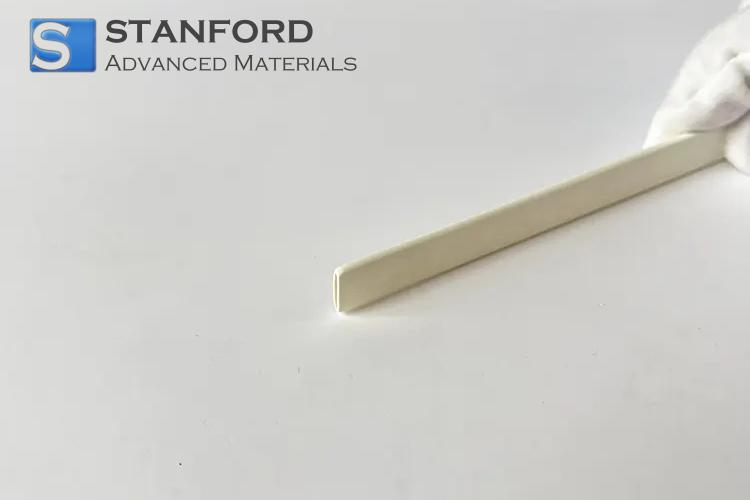
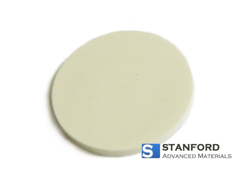
Fig. 1 Various Boron Nitride Ceramic Products
2 Detailed Process Principles and Workflow
2.1 Hot Pressed Boron Nitride - HPBN
The fabrication of hot-pressed boron nitride (HPBN) begins with high-purity hexagonal boron nitride (h-BN) powder as the primary raw material. To enhance sintering densification, minor additions of sintering aids, typically boron oxide (B2O3), calcium oxide (CaO), or aluminum oxide (Al2O3), are incorporated into the powder mixture. The core process involves loading the homogenized powder into a purpose-designed graphite die, followed by simultaneous application of elevated temperature (1700–2000°C) and uniaxial pressure (10–40 MPa) under inert atmosphere (typically nitrogen, N2, or argon, Ar) or vacuum conditions.
The densification mechanism during hot pressing involves synergistic physicochemical interactions: (1) thermal softening of h-BN particles at elevated temperatures, (2) pressure-induced particle sliding, rearrangement, and plastic deformation, and (3) liquid-phase formation from sintering aids at high temperatures. This liquid phase accelerates densification through dissolution-reprecipitation processes at particle surfaces and grain boundary sliding. The complete workflow encompasses precise powder blending, die loading, atmosphere control (via vacuum pumping or gas purging), simultaneous temperature/pressure ramping, isothermal-isobaric holding to achieve full densification, and controlled cooling/depressurization before demolding. While hot pressing yields near-net-shape components, subsequent machining operations (e.g., cutting, grinding) are often required to meet final dimensional tolerances.
HPBN products predominantly manifest as high-density bulk materials, including plates, rods, crucibles, nozzles, and specialized insulation components. The achievable geometries and dimensions are directly constrained by the design and load-bearing capacity of the graphite tooling system.
2.2 Pyrolytic Boron Nitride - PBN
Pyrolytic boron nitride (PBN) is fabricated via chemical vapor deposition (CVD) using gaseous precursors such as boron trichloride (BCl3) or boron tribromide (BBr3) and ammonia (NH3) as reactant gases. The process occurs within specialized deposition furnaces operated at temperatures ranging from 1400°C to 1900°C under pressures spanning low vacuum to atmospheric conditions. The deposition sequence commences with loading a cleaned substrate (typically high-purity graphite) into the reaction chamber, followed by vacuum pumping and introduction of precisely controlled precursor/carrier gas mixtures. Upon reaching the target deposition temperature through programmed heating, the precursor gases undergo thermal decomposition and recombination at the heated substrate surface, enabling atomic-scale material growth via the reaction: BCl3 + NH3 → BN + 3HCl.
The material growth mechanism follows a surface-reaction-dominated layer-by-layer accumulation process: gaseous molecules adsorb onto the substrate surface, migrate, and nucleate before forming BN crystalline structures through chemical bonding. Deposition layer density, crystallographic orientation, and growth rate are critically governed by four parameters:
- Substrate temperature (modulating surface reaction kinetics and atomic mobility)
- Reactor pressure (influencing gas molecule mean free path)
- Precursor gas flow ratios (determining reaction equilibrium and impurity levels)
- Substrate surface condition (roughness and crystallographic orientation affecting nucleation density).
Following controlled cooling, final products are classified into two categories: free-standing structures detached from sacrificial substrates via mechanical/chemical release, or conformal coatings directly deposited onto functional components. PBN products exhibit ultra-high purity (>99.99%) and non-porous microstructures, with characteristic morphologies including:
- Complex curved coatings (typically <500 μm thickness)
- Thin-walled self-supporting structures (tubes, crucibles, boats with millimeter-scale wall thickness)
- Enclosed geometries with intricate 3D profiles
While PBN enables deposition of complex configurations, its inherently slow growth rate results in exponentially increasing fabrication times for thick sections (>5 mm), rendering it economically less viable compared to bulk molding techniques like hot pressing for large-volume applications.

Fig. 2 Changes in The Mechanical Properties and Microstructure of Boron Nitride Blocks at Different Forming Temperatures
3 Core Process Characteristics and Comparison
3.1 Process Essence and Raw Material System
HPBN (Hot-Pressed Boron Nitride):
This method utilizes solid-state sintering technology. Starting with hexagonal boron nitride (h-BN) powder, densification occurs under high temperature and pressure. Sintering aids (such as B2O3 or CaO) promote densification by forming a liquid phase that reduces grain boundary energy, facilitating particle rearrangement and plastic flow.
PBN (Pyrolytic Boron Nitride):
This is a chemical vapor deposition (CVD) technique. Gaseous precursors (BCl3 or BBr3) react with NH3, enabling atomic-level deposition via surface chemical reactions (e.g., BCl3 + NH3 → BN + 3HCl). This process achieves high purity and eliminates the need for mechanical compaction.
3.2 Key Process Parameters
Table 1 Key Process Parameters Comparison of HPBN and PBN
|
Parameter |
HPBN (Hot-Pressed Boron Nitride) |
PBN (Pyrolytic Boron Nitride) |
|
Temperature Range |
1700-2000°C (solid-state diffusion dominated) |
1400-1900°C (surface reaction dominated) |
|
Pressure Conditions |
10-40 MPa (uniaxial mechanical pressure) |
Low vacuum to atmospheric pressure (no external pressure) |
|
Atmosphere Control |
N2/Ar inert atmosphere or vacuum |
Precisely controlled precursor + carrier gas mixture |
|
Time Scale |
Hours (during holding stage) |
Days (due to slow deposition rate for thickness buildup) |
3.3 Mechanism of Microstructure Formation
HPBN:
Densification originates from physical mechanisms:
- Particle sliding and rearrangement (driven by high pressure)
- Grain boundary diffusion (facilitated by elevated temperature)
- Liquid-phase assisted dissolution-reprecipitation (enabled by sintering aids)
The resulting material is a polycrystalline aggregate with grain sizes of approximately 5-20 μm.
PBN:
Growth is governed by chemical kinetics:
- Adsorption of gas-phase molecules onto the substrate
- Surface migration and nucleation (highly temperature-sensitive)
- Chemical bonding forms layered structures
The product features highly aligned columnar grains exhibiting through-thickness growth.

Fig. 3 XRD Patterns and Microstructure of The Bulk Ceramics Prepared Through SPS.
3.4 Product Performance and Geometric Characteristics
Table 2 Comparison of Hot-Pressed (HPBN) and Pyrolytic Boron Nitride (PBN) Properties
|
Property |
HPBN (Hot-Pressed Boron Nitride) |
PBN (Pyrolytic Boron Nitride) |
|
Purity |
99.5-99.9% (contains sintering aid residues) |
>99.99% (impurity-free vapor deposition) |
|
Density |
1.8-2.0 g/cm3 (residual microporosity) |
2.2 g/cm3 (theoretical density, pore-free) |
|
Formability |
Limited to simple shapes via mold constraints |
Complex curved coatings / Free-standing thin-walled structures |
|
Typical Thickness |
Millimeters to centimeters (no inherent limitation) |
Coatings: <500 μm Free-standing: <3 mm |
|
Anisotropy |
Weak (random grain orientation) |
Strong (c-axis perpendicular to substrate) |
3.5 Technical and Economic Comparison
HPBN excels in cost-effective mass production of thick-section components (e.g., crucibles, insulating plates) with relatively low equipment investment (hot presses vs. CVD systems). Conversely, PBN enables ultra-high-purity, contamination-free environments essential for semiconductor applications and achieves near-net-shape fabrication of complex thin-walled structures, significantly reducing material waste.
Both technologies face inherent constraints: HPBN struggles with manufacturing sub-1mm thin-walled components due to brittle fracture risks during demolding, while PBN experiences exponential cost escalation beyond 5mm thickness due to its slow deposition rate (~20 μm/h).
Table 3 Comparative Fabrication Processes: Hot-Pressed Boron Nitride (HPBN) Sintering vs. Pyrolytic Boron Nitride (PBN) Chemical Vapor Deposition
|
Comparison Dimension |
Hot-Pressed Boron Nitride (HPBN) |
Pyrolytic Boron Nitride (PBN) |
|
Process Category |
Solid-state sintering |
Chemical Vapor Deposition (CVD) |
|
Raw Material Form |
h-BN powder + sintering additives |
BX₃ (X=Cl/Br) + NH3 gas precursors |
|
Densification Mechanism |
Mechanical pressure (10-40 MPa) |
Surface chemical reaction energy |
|
Core Temperature Range |
1700-2000°C |
1400-1900°C |
|
Microstructure Formation |
Particle rearrangement + grain boundary diffusion |
Adsorption-migration-nucleation-bonding sequence |
|
Key Equipment |
Hot-pressing furnace |
Vacuum CVD reactor |
|
Product Purity |
99.5-99.9% |
>99.99% |
|
Geometric Capabilities |
Thick monolithic blocks (≥1 cm) Simple shapes |
Complex curved coatings Free-standing thin shells/tubular structures |
|
Thickness Limitations |
Lower limit ~1 mm (brittleness constraint) |
Upper limit ~5 mm (economic viability) |
|
Typical Applications |
Molten metal crucibles, high-temperature insulators |
Semiconductor chamber liners, MBE source boats |
4 Comparative Analysis of Material Properties
Although both Hot-Pressed Boron Nitride (HPBN) and Pyrolytic Boron Nitride (PBN) belong to the hexagonal boron nitride system, their microstructural differences dictate fundamentally divergent macroscopic properties. HPBN, formed via high-temperature/high-pressure sintering, exhibits randomly oriented grains that create a polycrystalline structure containing trace isolated closed pores (0.5-3 μm) with densities of 1.8-2.0 g/cm3. Residual sintering aids (e.g., B2O3) limit its purity to 99.5-99.9%. In contrast, PBN—produced through chemical vapor deposition—develops columnar grains growing normal to the substrate, yielding a fully dense (2.20-2.25 g/cm3), monophasic structure exceeding 99.99% purity without sintering additive incorporation.
4.1 Thermal and Electrical Properties
The columnar crystal structure of PBN endows it with extreme anisotropic thermal conductivity properties: the thermal conductivity along the deposition plane (a-b plane) direction reaches as high as 150–220 W/(m·K), approaching the theoretical limit of h-BN single crystals; whereas the thermal conductivity perpendicular to the deposition plane (c-axis) direction drops sharply to 1–3 W/(m·K), forming a natural thermal barrier. In contrast, HPBN exhibits isotropic thermal conductivity (25–60 W/(m·K)) due to its disordered grain arrangement, and its grain boundaries significantly reduce thermal conductivity through phonon scattering. Both materials exhibit excellent electrical insulation properties, with volume resistivities exceeding 10^13 Ω·cm. However, PBN, due to its pore-free structure, has a slightly higher breakdown strength (40–50 kV/mm) than HPBN (30–40 kV/mm).
4.2 Vacuum and Chemical Stability
The fully dense structure of PBN enables it to achieve an outgassing rate as low as 5×10^-11 Torr·L/(s·cm^2) in ultra-high vacuum environments (<10^-10 mbar), which is 1-2 orders of magnitude lower than that of HPBN, making it the preferred choice for core components in semiconductor epitaxial equipment. In terms of chemical inertness, both materials resist corrosion from molten metals (Al, Cu, Au) and non-oxidizing acids. However, PBN demonstrates superior resistance to molten alkali corrosion (e.g., NaOH) due to the absence of impurity phases. High-temperature oxidation threshold tests indicate that PBN remains stable up to 850°C in dry air, outperforming HPBN's 800°C threshold. This difference stems from the accelerator at HPBN's grain boundaries, which accelerates the oxidation process.
4.3 Mechanical Properties and Machinability
The flexural strength (30–100 MPa) and fracture toughness (2.5–3.5 MPa·m^1/2) of HPBN confer on its graphite-like machinability, enabling the production of complex geometries through conventional mechanical processing. Although PBN exhibits higher strength (120–180 MPa) in the a-b plane direction, its layered structure results in brittle delamination along the c-axis direction (fracture toughness of only 1.0–1.8 MPa·m^1/2), with microhardness (350–400 kgf/mm2) approximately 1.5 times that of HPBN. This contradictory combination of high hardness and low toughness makes PBN nearly impossible to machine via turning or milling, and it can only be directly formed through precision grinding or deposition processes.
Table 4 Comparison of Key Performance Parameters
|
Property |
Hot-Pressed Boron Nitride (HPBN) |
Pyrolytic Boron Nitride (PBN) |
|
In-Plane Thermal Conductivity |
25-60 W/(m·K) |
150-220 W/(m·K) |
|
Through-Thickness Thermal Conductivity |
25-60 W/(m·K) |
1-3 W/(m·K) |
|
Vacuum Outgassing Rate |
~10^-9 Torr·L/(s·cm2) |
<5×10^-11 Torr·L/(s·cm2) |
|
Machinability |
Good (turning/drilling applicable) |
Poor (limited to cutting/grinding) |
4.4 The Physical Essence of Performance Differences
The pronounced anisotropy in PBN arises from its highly oriented columnar grain structure: strong covalent bonding within the a-b planes facilitates high thermal conduction pathways, while weak van der Waals forces along the c-axis direction cause significant thermal resistance. Conversely, HPBN exhibits uniform properties due to random grain stacking. Its isolated micropores slightly compromise mechanical strength but enable machinability. Notably, PBN's coexistence of high in-plane strength (parallel to deposition surface) and weak through-thickness integrity fundamentally reflects hexagonal boron nitride's layered crystal structure, where basal plane covalent bonding exhibits over two orders of magnitude greater strength than interlayer van der Waals forces.
4.5 Engineering Selection Principles
In semiconductor ultra-high vacuum systems, the PBN crucible proves indispensable due to its ultra-low outgassing and high purity. For applications requiring mechanical load-bearing capability or complex shaping (e.g., molten salt electrolysis cell linings), HPBN offers greater processing advantages. This performance divergence originates from structural control precision: HPBN represents the performance compromise inherent to conventional powder metallurgy, whereas PBN demonstrates vapor deposition's capacity to maximize intrinsic material properties. Future advancements require addressing PBN's processing limitations or enhancing HPBN's thermal conductivity through grain-orientation control techniques.

Fig. 4 Pyrolytic Boron Nitride VGF Crucible
5 Typical Application Scenario Analysis
5.1. Advantageous Fields of Hot-Pressed Boron Nitride (HPBN)
HPBN demonstrates irreplaceable value in applications requiring isotropic properties, machinability, and cost efficiency: Large-scale high-temperature containers like GaAs/GaP semiconductor melt crucibles (>300 mm diameter) and aluminum alloy casting distribution pans leverage its uniform thermal expansion coefficient (3.5-4.5×10^-6/°C) to withstand thermal cycling stresses, while substantial wall thicknesses (≥20 mm) ensure molten material containment. For complex functional components, HPBN enables machined cooling channels in plasma arc chamber linings that are resistant to arc erosion, and achieves Ra 0.4 μm surface finishes on glass molding dies to prevent adhesion. In cost-sensitive applications such as welding nozzles or heat treatment fixtures, HPBN's sintered manufacturing reduces costs by 60-80% compared to PBN, with controlled porosity (<3%) maintaining functional performance. A notable case involves polycrystalline silicon ingot furnace insulation supports (flexural strength ≥80 MPa) exhibiting <0.5 mm deformation after 2000 hours at 1560°C, significantly outperforming graphite alternatives.
PBN dominates high-end applications through extreme purity (>99.99%), intrinsic densification, and engineered thermal anisotropy. In ultra-high-purity semiconductor manufacturing, MBE source boats prevent metal contamination (Al, Fe), while PBN's outgassing rate <5×10^-11 Torr·L/(s·cm^2) preserves film integrity. Vertical Bridgman (VB) GaAs crystal growth achieves carbon impurity levels <10^15 atoms/cm^3 using PBN crucibles. Critical vacuum systems like synchrotron beamline collimators (10^-10 Pa) utilize PBN liners to prevent hydrocarbon desorption, and mass spectrometer ion sources exploit their low sputtering yield (<10^-4 atoms/ion). Directional thermal management includes laser diode heat sinks where 2mm PBN substrates deliver >200 W/(m·K) in-plane conductivity while limiting c-axis conduction to 1.5 W/(m·K), and continuous casting monitor shields maintaining cold ends <200°C despite 1600°C hot zones. PBN's near-net-shaping capability produces thin-walled structures like RF plasma generator tubes (0.8-1.2 mm thickness, as-deposited Ra<0.1 μm), ensuring plasma uniformity without post-processing. An ion implanter case study using PBN arc chambers (99.995% purity) reduced silicon wafer metal contamination to 5×10^9 atoms/cm2, two orders of magnitude lower than alumina components.
Table 5 Selection Decision Mechanism
|
Selection Dimension |
HPBN Preferred Conditions |
PBN Preferred Conditions |
|
Purity Requirement |
≤99.9% acceptable |
>99.99% (essential to avoid trace contamination) |
|
Vacuum Level |
High vacuum (HV, 10^-3~10^-7 Pa) |
Ultra-high/extreme vacuum (UHV/XHV, <10^-8 Pa) |
|
Thermal Management |
Isotropic heat distribution |
Engineered anisotropy (a-b plane vs. c-axis >100× difference) |
|
Geometric Complexity |
3D complex structures (requiring machining) |
Thin-walled shells/tubular structures (direct deposition forming) |
|
Cost Constraint |
Medium-low budget |
Premium performance justified |
5.2 Deep Interconnectivity of Application Scenarios
Intrinsic Purity Advantage:
PBN's dominance in semiconductor applications originates from its inherent purity. The vapor deposition process avoids introducing elements beyond B and O (e.g., Ca, Al) present in sintering aids, whereas even 0.1% B2O3 in HPBN can volatilize above 1400°C and contaminate InP epitaxial layers.
Thermal Management Innovation:
PBN's thermal anisotropy enables revolutionary heat dissipation architectures. In kilowatt-class laser modules, PBN substrates increase heat dissipation efficiency by 300% while limiting temperature rise in thermally sensitive optics to <5°C - a significant improvement over conventional AlN substrates, which typically cause >30°C temperature increases.
 And Perpendicular to The Deposition Plane (C-Direction) Differs by A Factor of About 20, Making It an Ideal Material for Manufacturing Crystal Growth Crucibles. Therefore, PBN Crucibles Are Also a Popular Choice in The Field of GaAs Crystal Growth.")
Fig. 5 The CVD Process Also Yields PBN A Nearly Perfect Layered Structure, As Shown in The Figure Below. This Results in Anisotropic Thermal Conductivity—The Thermal Conductivity in The Deposition Direction (A-Direction) And Perpendicular to The Deposition Plane (C-Direction) Differs by A Factor of About 20, Making It an Ideal Material for Manufacturing Crystal Growth Crucibles. Therefore, PBN Crucibles Are Also a Popular Choice in The Field of GaAs Crystal Growth.
Failure Mode Mitigation:
HPBN's application in plasma arc chambers leverages its uniform wear characteristics. The polycrystalline structure enables isotropic sputter erosion rates (0.1-0.3 mm/1000h), while PBN may experience layer-by-layer delamination under ion bombardment due to its anisotropic layered structure.
6 Conclusion
The performance divergence between Hot-Pressed Boron Nitride (HPBN) and Pyrolytic Boron Nitride (PBN) stems from their distinct manufacturing processes. HPBN, formed via powder sintering, develops a polycrystalline structure with isotropic properties and good machinability at lower costs. However, residual porosity (0.5-3%) and sintering additives limit its purity to ≤99.9%, resulting in higher vacuum outgassing (~10^-8 Torr·L/(s·cm^2)). In contrast, PBN grows columnar grains through chemical vapor deposition, achieving >99.995% purity and outgassing rates below 5×10^-11 Torr·L/(s·cm^2). Its thermal conductivity exhibits pronounced anisotropy, reaching 220 W/(m·K) in the a-b plane but only 2 W/(m·K) along the c-axis, though weak interlayer bonding causes machining brittleness.
Application selection depends on performance boundaries:
- HPBN excels in large molten crucibles (e.g., copper smelting) and plasma chamber liners requiring complex machining or cost sensitivity
- PBN remains irreplaceable for MBE crucibles, ion implanter arc chambers, and laser heat sinks demanding >99.99% purity or directional thermal management
The selection framework prioritizes three critical parameters:
- Vacuum Requirements: PBN mandatory for pressures <10^-8 Pa
- Thermal Management: PBN is essential when directional conductivity is needed (>200 W/(m·K) in-plane with <3% through-thickness leakage)
- Cost Threshold: PBN is favored in scenarios where performance demands outweigh machining ease and cost sensitivity.
Future breakthroughs must address fundamental limitations: HPBN requires enhanced in-plane conductivity (currently <40 W/(m·K)), while PBN needs improved c-axis toughness. Hybrid structures (e.g., PBN coatings on HPBN substrates) present viable solutions, having already validated 50% lifetime improvement in semiconductor carrier trays.
To fully leverage the unique advantages of both HPBN and PBN, consistent access to high-quality, application-specific materials is paramount. Stanford Advanced Materials (SAM) stands at the forefront of this supply chain, offering an extensive range of boron nitride products tailored to meet the stringent demands of semiconductor, aerospace, and industrial sectors. Beyond product provision, SAM delivers expert technical support and customized solutions, enabling material engineers and designers to optimize performance and accelerate innovation. Partnering with trusted suppliers like SAM ensures that the transformative potential of boron nitride polymorphs is fully realized across diverse and challenging technological frontiers.、
 Chin Trento